Our current research efforts, in short:
April 12, 2020
Wearable electronic devices integrating with the natural environment and human experience have been receiving increasing attention. Energy conversion devices that can convert ambient energy into electricity are eagerly desired for self-powered wearable devices. In the past decade, several types of flexible energy conversion devices have been developed on the basis of piezoelectricity, electrostaticity, and triboelectricity, but these devices are usually inefficient and costly. Flexible thermoelectric (TE) devices may satisfy the requirements because they can directly convert human body heat into electricity. Unfortunately, the development of flexible TE devices suffers from the absence of TE materials with both promising TE properties and flexibilities. Traditional inorganic TE materials normally exhibit poor mechanical properties, which may result in device failure, because they are brittle and prone to rupture under tensile, compression, or bending load. Organic TE materials can be flexible, but they display poor electrical properties and low power factors. Organic/inorganic TE composites have the combined advantages of flexible polymers and inorganic TE materials. However, the flexibility of the TE device made from organic/inorganic composites is mainly realized by the flexible substrate but not the TE material itself. The inorganic component, which contributes to the TE performance of the device, displays poor flexibility and must be deposited as a thin film (usually only several micrometers thick) on the flexible organic substrate. This results in not only complicated, time-consuming, and costly production processes but also uncontrollable device performance because of the problems inhomogeneity and thickness variation of the thin film. Research and development of freestanding flexible TE materials are urgently needed to realize a self-power supply for wearable electronic devices.
Reference:
1. He S, Li Y, Liu L, et al. Semiconductor glass with superior flexibility and high room temperature thermoelectric performance[J]. Science advances, 2020, 6(15): eaaz8423.
Flexible Thermoelectric Materials and Devices
Thin Films Deposited by Atomic Layer Deposition
April 12, 2021
Atomic layer deposition (ALD) appears to be one of the most promising techniques due to its simplicity, reproducibility, and the high conformality of the obtained films. As a matter of fact, ALD was already chosen by the microelectronic industry as the technique of choice for the fabrication of next-generation metal-insulator-metal capacitors in DRAMs and to deposit gate oxide in CMOS transistors. High aspect ratio structures, nanoparticles, nanowires, nanotubes, soft materials, biological materials can be precisely coated by ALD. The obtained heterostructures have a large range of applications, such as in catalysis, microelectronics, energy storage and conversion, sensing, etc.
Reference:
1. He S, Bahrami A, Zhang X, et al. Atomic layer deposition and characterization of Bi1Se1 thin films[J]. Journal of the European Ceramic Society, 2023, 43(11): 4808-4813.
2. He S, Bahrami A, Zhang X, et al. Low-temperature ALD of highly conductive antimony films through the reaction of silylamide with alkoxide and alkylamide precursors[J]. Materials Today Chemistry, 2023, 32: 101650.


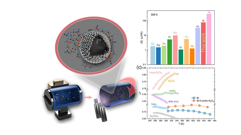
Powder Atomic Layer Deposition Enhanced Thermoelectric Performance
May 30, 2021
As a layer-by-layer deposition technique, atomic layer deposition (ALD) is known for its unique capability of depositing highly uniform films in a controlled manner. Compared with traditional CVD methods, the precursors in ALD are always kept separated and pulsed alternatively into the chamber with a purging phase in between. Thanks to the controlled layer-by-layer growth, ALD can uniformly coat any structure: from planar substrates to 3D structures, trenches, and holes. The thickness control can be down to the atomic level, enabling the deposition of extremely thin films, even only a few atoms thick. This remarkable feature indicates that the ALD method can be effectively applied on powder surfaces. The concept of powder ALD (PALD) can be divided into two procedures: preparing a thermoelectric powder with adequately tiny size and coating the shell materials with a rotation process. The rotation process, combined with the small size of the powder particles, ensures a uniform coating even with a few cycles. Briefly, the powder size (d) and the potential energy barrier must be specifically designed to satisfy the relationship that τp (phonon momentum relaxation length) < d < τe (electron momentum relaxation length); in this manner, S will be improved without significantly decreasing σ, resulting in a substantial net improvement of PF. Additionally, a large reduction in thermal conductivity can be achieved by depositing a few layers of specific materials on the interfaces of the TE material particles.
Reference:
1. He S, Lehmann S, Bahrami A, et al. Current State‐of‐the‐Art in the Interface/Surface Modification of Thermoelectric Materials[J]. Advanced Energy Materials, 2021, 11(37): 2101877.
2. He S, Bahrami A, Zhang X, et al. Effect of Powder ALD Interface Modification on the Thermoelectric Performance of Bismuth[J]. Advanced Materials Technologies, 2021, 2100953.
3.He S, Yang J, Bahrami A, et al. Surface Modification of Bismuth by ALD of Antimony Oxide for Suppressing Lattice Thermal Conductivity[J]. ACS Applied Energy Materials, 2022, 5(4): 4041-4046.


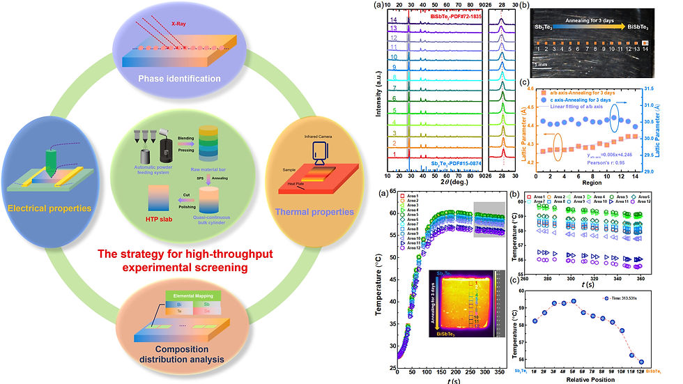
High throughput Method to Screen High Thermoelectric Performance for Bulk Materials
Sep 1, 2021
Searching for new materials is of great significance due to the persistent demand for advanced materials in modern society, but the efficiency of material discovery has long been limited by the traditional Edisonian trial and error approach. Recently, high-throughput (HTP) techniques have attracted intensive efforts owing to their ability in speeding up the research and development of novel materials. HTP prediction based on theoretical calculation and machine learning has made remarkable progress and achieved great success in a variety of materials. For example, simultaneous advances in theoretical calculation, integrated databases, and machine learning have initiated new revolutions of materials development in the field of superconducting and fluorescent materials. However, HTP experiments, particularly for bulk samples, have lagged behind. HTP experiments are important for the searching for new materials because they can not only verify the result of HTP prediction but also help to calibrate and enrich computational models and material databases by providing experimentally measured data, which further promotes the development of HTP predication in turn. Thus, HTP experiments are capable of launching material design into a new era.
Reference:
1. Pu H Y, Xie R Q, Peng Y, et al. Accelerating sample preparation of graded thermoelectric materials using an automatic powder feeding system[J]. Advances in Manufacturing, 2019, 7(3): 278-287.
2. You L, Li Z, Ma Q, et al. High thermoelectric performance of Cu-doped PbSe-PbS system enabled by high-throughput experimental screening[J]. Research, 2020, 2020.
3. He S, Yang Y, Li Z, et al. A general strategy for high-throughput experimental screening of promising bulk thermoelectric materials[J]. Science China Materials, 2021, 64(7): 1751-1760.